
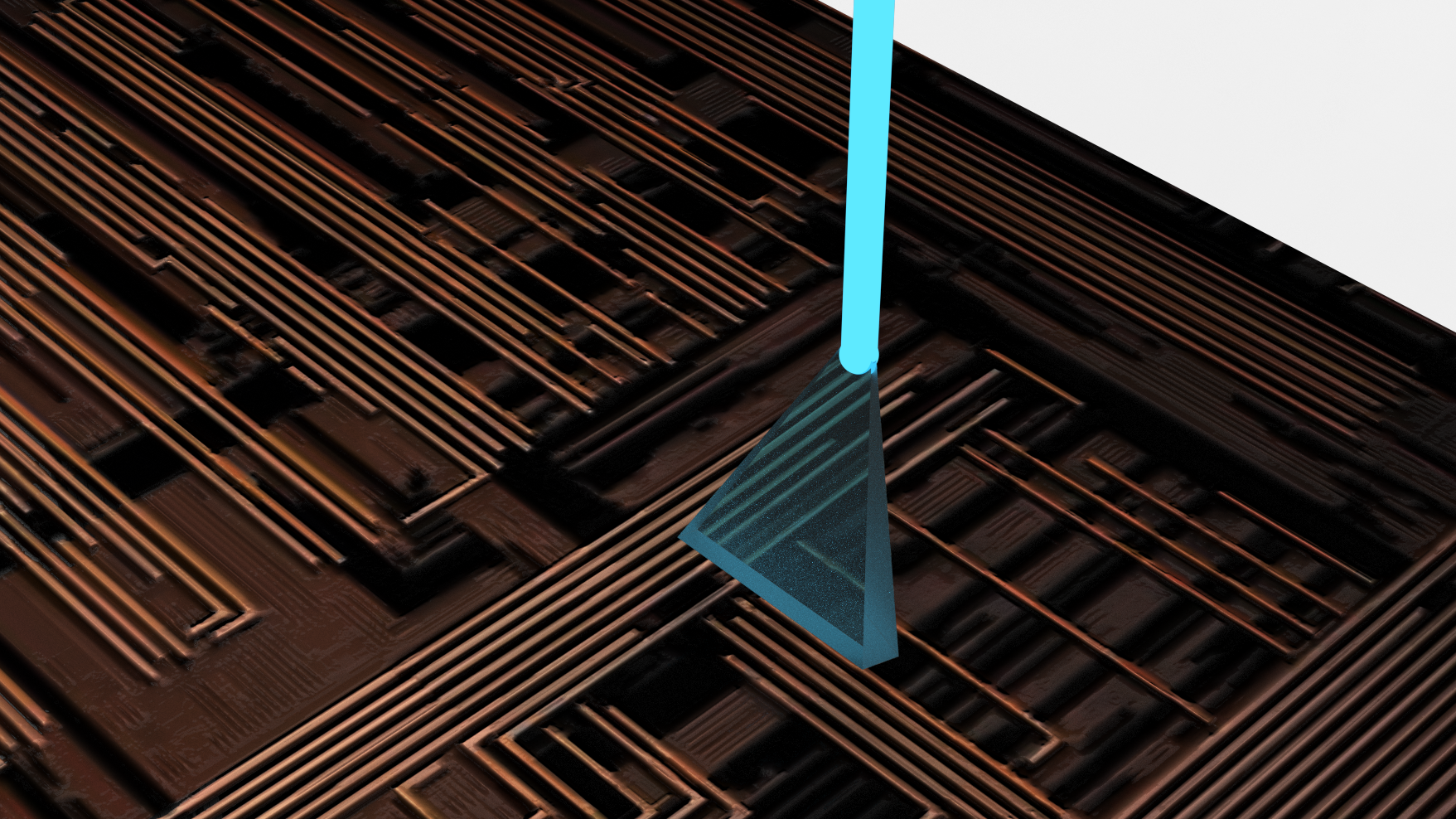
Semiconductor & Electronics
Find the failure without destroying the evidence.
Modendo brings high-resolution optical access into confined regions of backside power-delivery devices and advanced 3D packages—helping failure-analysis teams reach answers conventional laser tools cannot.
THE CHALLENGE
The chips advancing AI are becoming harder to inspect.
Backside power delivery, stacked dies, and dense chiplet architectures place critical transistors, interconnects, and interfaces behind metal and between layers.
Conventional optical tools require a clear line of sight. Reaching these hidden regions can demand extensive sample preparation that risks removing the very evidence needed to understand the failure.
THE MODENDO SOLUTION
Bring the optical path to the failure.
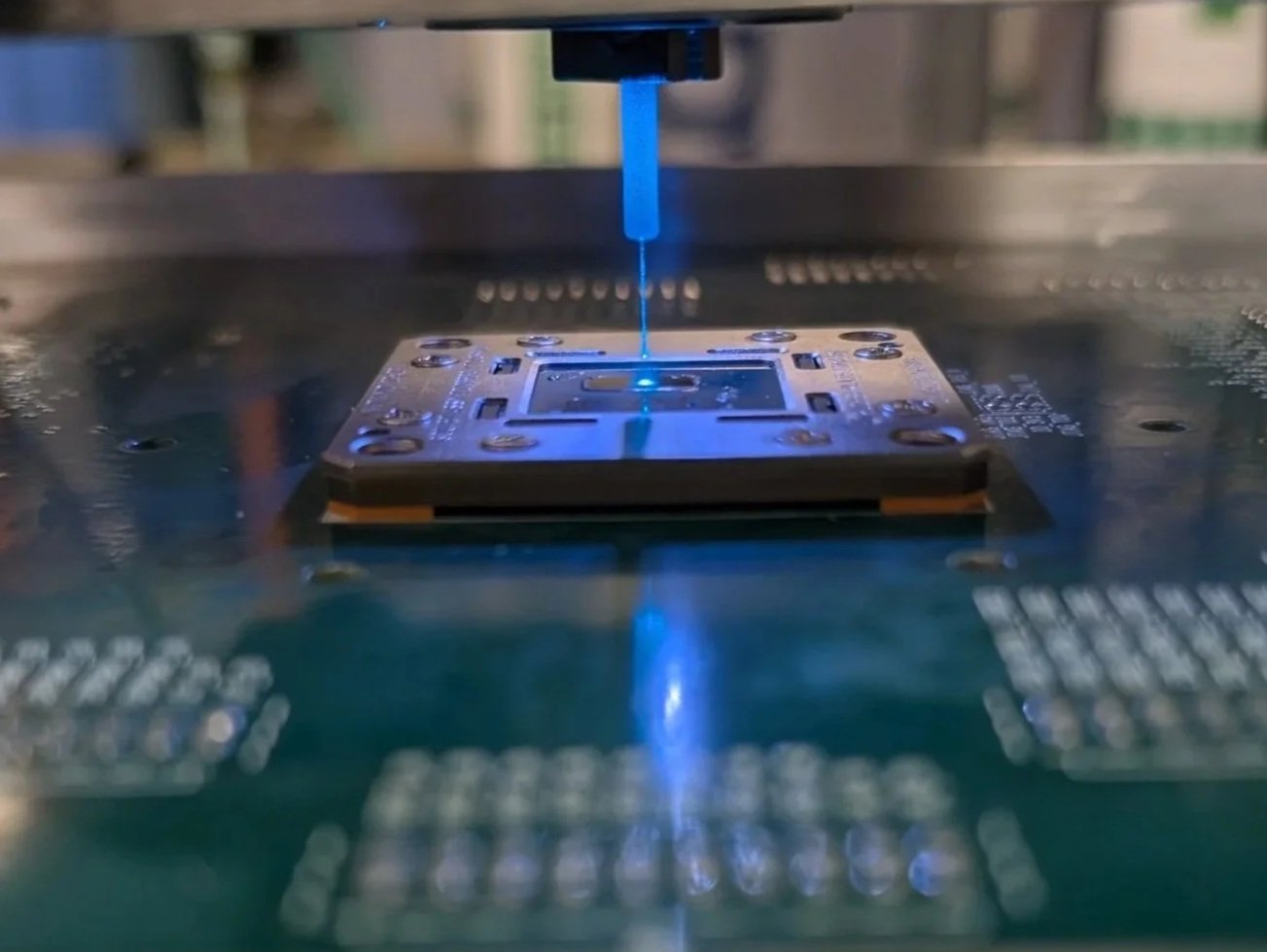
Modendo uses a flexible fiber probe approximately 100 µm wide to deliver and collect light inside confined chip structures.
The system enables localized imaging, targeted laser illumination, and optical fault isolation with less clearing of packaging and metallization—preserving more of the device for continued analysis.
Accessing deeper value for your team.
For Failure-Analysis Teams
Reach hidden failure sites, preserve defect evidence, and move from observation to root cause with greater confidence.
For Packaging and R&D Leaders
Gain a new way to investigate advanced architectures, resolve development issues, and protect learning cycles as designs become more complex.
For Tool and Channel Partners
Add a differentiated optical capability that can complement existing microscopy, test, and failure-analysis workflows.
USE CASES
Built for next-generation device architectures.
-
Access transistor regions hidden behind backside metal and power-delivery structures.
-
Navigate between stacked dies and chiplets to inspect buried interfaces and interconnects.
-
Deliver targeted illumination into confined regions, including Laser Assisted Device Alteration (LADA) workflows on operating devices.
-
Support localized imaging and material analysis where conventional free-space optics lose line of sight.
IMAGING RESULTS
See what the probe can reach.
Imaging at the Point of Access
Reflection imaging captured at multiple working planes near the fiber tip.
Raw Signal to Reconstructed Image
A side-by-side comparison showing how computational processing reveals clearer structural information.
Navigation Through Confined Geometry
Video of the probe moving through 500 µm access openings to reach otherwise inaccessible regions.
TECHNICAL CAPABILITIES
Engineered for confined optical access.
Probe diameter on the order of 100 µm
Flexible probe geometry
High-numerical-aperture optics
Localized, high-resolution reflection imaging
Holographic laser scanning
Targeted photo-illumination
Minimal moving components at the point of access
Computational image reconstruction
Integration potential with existing FA systems
Adaptable pathways for IR, Raman, hyperspectral, and 3D surface measurements
Bring us the access problem.
If a critical region is blocked from conventional optical inspection, let’s determine whether Modendo can create a path to it.