
Semiconductor Inspection
The rise of advanced 3D packaging has enabled unprecedented integration densities but also introduced significant challenges for failure analysis. Conventional nondestructive methods such as optical microscopy are constrained by line-of-sight limitations, while X-ray and CT imaging often lack the surface sensitivity or material specificity to resolve subtle defects.
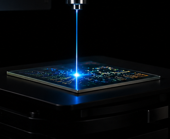
The Modendo ultrathin microendoscope provides a transformative solution by delivering direct optical access into confined internal regions of complex 3D assemblies. With probe diameters on the order of ~100 µm, high-numerical-aperture optics, and flexible maneuverability, the system enables localized, high-resolution imaging and targeted photo-illumination of hidden joints, interconnects, and interfaces behind metal layers or deep within stacked structures.
Optical FA inspection of electronics at a tip of a 100um needle
Video showing to different imaging planes: 150µm and 10µm far from the tip of the probe (Raw data)

Raw data signal vs the deconvolved image using the variant system PSF
Navigation of Modendo reflection system probe through 500µm diameter apertures
Beyond simple visualization, the Modendo platform delivers holographic laser scanning that allows optical inspection and spectroscopy to support deeper analysis. The probe can be coupled with Raman, hyperspectral, or IR modalities for in-situ material characterization, and it can also be adapted for 3D topographic reconstructions of buried surfaces. By directly addressing the two-side metal challenge, Modendo allows defect inspection and material analysis with only minimal clearing of packaging and metallization. This reduces dependence on destructive cross-sectioning, accelerates root-cause identification, and preserves valuable devices for subsequent electrical or reliability testing.